JTAG Port: Difference between revisions
| (12 intermediate revisions by the same user not shown) | |||
| Line 1: | Line 1: | ||
''' Thanks to rdk, the JTAG port has been identified - this page is no longer required ''' | |||
Bottom view of Barracuda module with probable JTAG pins: | |||
. | |||
. O ??? O TMS/TDI | |||
. | |||
. | |||
. O TDI/TMS | |||
. | |||
. | |||
. O ??? O ??? | |||
= Diagnostic = | = Diagnostic = | ||
| Line 5: | Line 21: | ||
JTAG consists of 4 or 5 pins: | JTAG consists of 4 or 5 pins: | ||
* TRST - A Reset line | * TRST - A Reset line. | ||
* TDI - Data In | * TDI - Data In | ||
* TDO - Data Out | * TDO - Data Out | ||
| Line 20: | Line 36: | ||
* TCK: Burst Clock for period of test | * TCK: Burst Clock for period of test | ||
* TDI: | * TDI: 111111111111111111 | ||
* TMS: 011111011000000000 | * TMS: 011111011000000000 | ||
| Line 31: | Line 47: | ||
If the input pins are connected correctly, some data should be seen on TDO as the instruction register last two bits are always '01'. | If the input pins are connected correctly, some data should be seen on TDO as the instruction register last two bits are always '01'. | ||
== Results == | |||
Assuming that TCK and TMS are on: J1,J2,J4 and/or J5, and that TDO is on pr5, pr15 or j3 - walked the above test pattern throug all pin combinations with no output change seen at all. | |||
Assuming that TCK and TMS are on: J1,pr6 and/or pr7, and that TDO is on pr5, pr15 or j3 - walked the above test pattern throug all pin combinations with no output change seen at all. | |||
It is possible that j3 is actually nreset for the module. | |||
Latest revision as of 19:30, 2 September 2007
Thanks to rdk, the JTAG port has been identified - this page is no longer required
Bottom view of Barracuda module with probable JTAG pins:
.
.        O ???        O TMS/TDI
.
.
.              O TDI/TMS
.
.
.             O ???    O ???
Diagnostic
Presently, a possible location for the JTAG port has been identified, but which pin is which has not.
JTAG consists of 4 or 5 pins:
- TRST - A Reset line.
- TDI - Data In
- TDO - Data Out
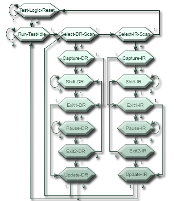
- TMS - The Mode Select pin, which actually drives the JTAG TAP Controller around a simple state machine.
- TCK - Clock
And Is Driven by a State Machine
Pin identification without risk of re-programming
TDO will have to be identified by impedence / voltage level testing.
- TCK: Burst Clock for period of test
- TDI: 111111111111111111
- TMS: 011111011000000000
1) TDI & TMS Change on TCK falling. 2) The '11111' of TMS forces the state machine to reset. 3) The '01100' of TMS forces it into the Shift-IR state. 4) The '00000000' of TMS forces the TDI in, and the Current Instruction Out.
If the inputs pins are connected incorrectly, the worst that can happen is '0' can be clocked into TMS twice, which should force the machine to stay in it's Run-Test/Idle state, and no damage can occur.
If the input pins are connected correctly, some data should be seen on TDO as the instruction register last two bits are always '01'.
Results
Assuming that TCK and TMS are on: J1,J2,J4 and/or J5, and that TDO is on pr5, pr15 or j3 - walked the above test pattern throug all pin combinations with no output change seen at all.
Assuming that TCK and TMS are on: J1,pr6 and/or pr7, and that TDO is on pr5, pr15 or j3 - walked the above test pattern throug all pin combinations with no output change seen at all.
It is possible that j3 is actually nreset for the module.
